I got this device on ebay for $10, it was sold as not tested. It was non functional. Dlink has since resued the DI-524 model number so finding information about it is a challenge. Date codes on most of the parts are all in the mid 1998’s this would have been a pricey device in its day.
I think it was desigend by “Argus Technologies Co Ltd” Taiwan judging by the bios dump and the FCC listing for its sister product and the styling of the user manual. The board is labled PN:AGS9884, on the rear of the board “M4954-B 9847”

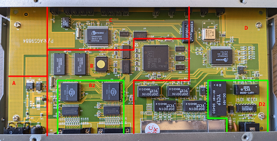
Lets talk about the different areas on the PCB
A – Power Control
4 Layer board?
B – AMD N80C188-25 16bit Microprocessor
External Logic – Address Translation
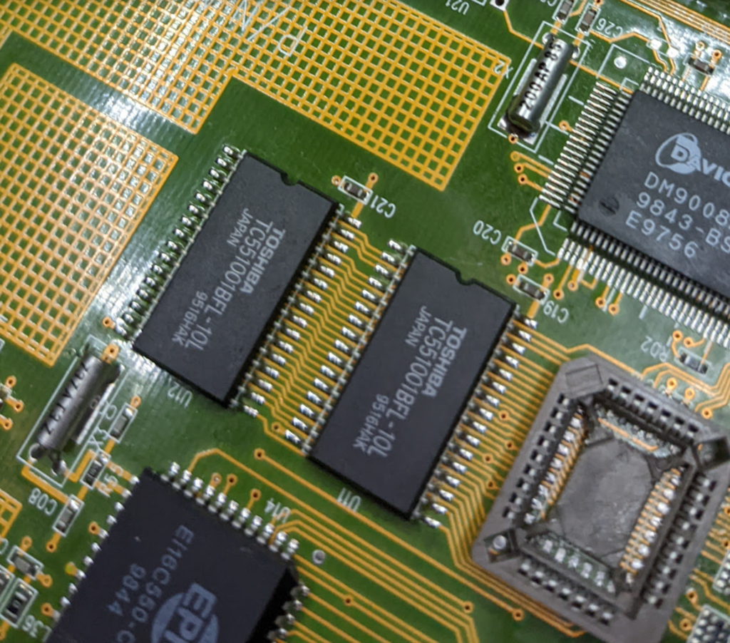
External Ram – TC551001BPL-10L (32pin SOP 100ns Static RAM)
External ROM – AM29F002T 265Kb (32pin PLCC)
B1 – Epic Hi16c550 FIFO UARTS
HIN238CB Transceivers
C – Davicom DM9008 ISA Plug and Play Super Ethernet Controller
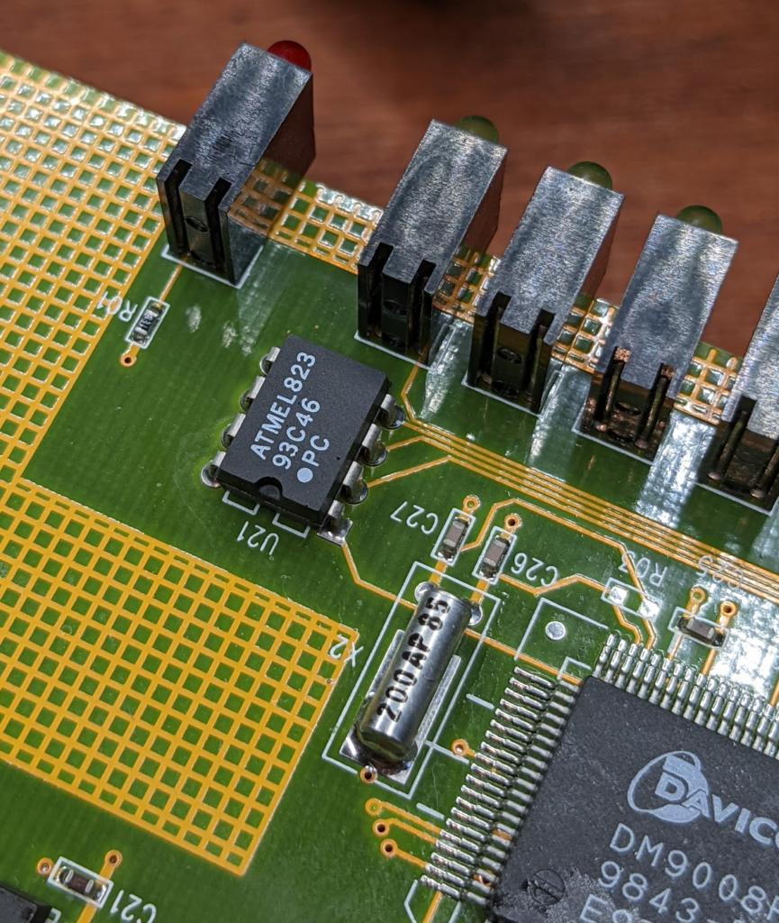
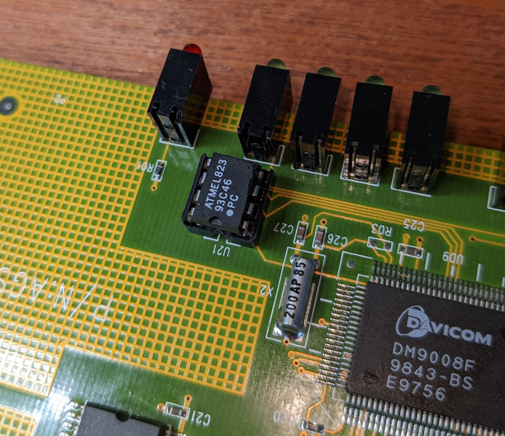
AT93c46 Serial EEPROM
D – Davicom DM9081 10BAST-T Hub Controller
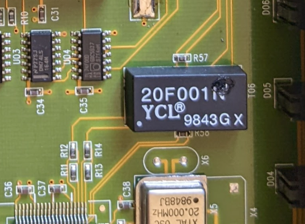
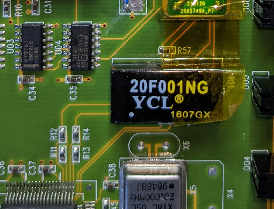
YCL 20F001N Magnetics
D2 – BNC MAU
URLS
https://web.archive.org/web/20010106193900/http://www.dlink.com.au/products/routers/di5xx/
Unhacking it?
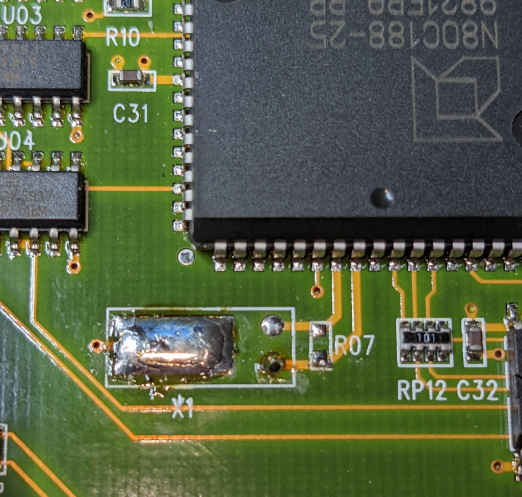
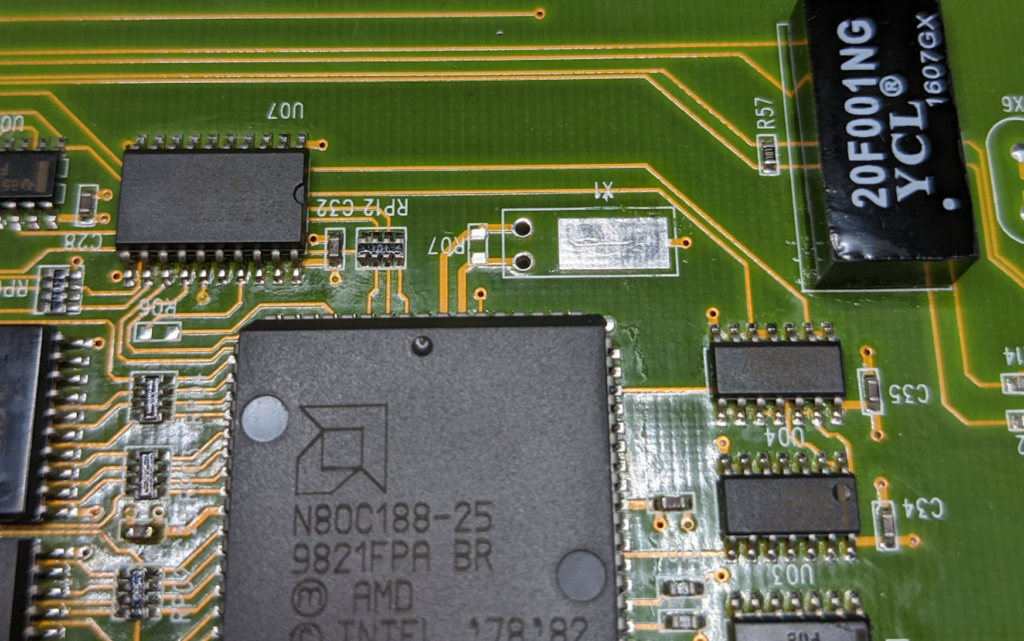
Was it a factory bodge or is it a user hack? This came with a 014 50Mhz clock can hastely soldered underneith, it looked a bit weird
The 186/188 CPU is a 25Mhz part so it can run up to that speed so you would need to provide 50Mhz to run the CPU at 25MHz.
I’m not sure you get small crystals that go that fast?…. plus it might not need to go that fast either, the memory parts are only 100ns so thats 10MHz, ie 20Mhz crystal.
……and the pcb layout dosent look quite right to me with a resistor bridge across the crystal pins so it could have been a factory bodge allbeith poor installation
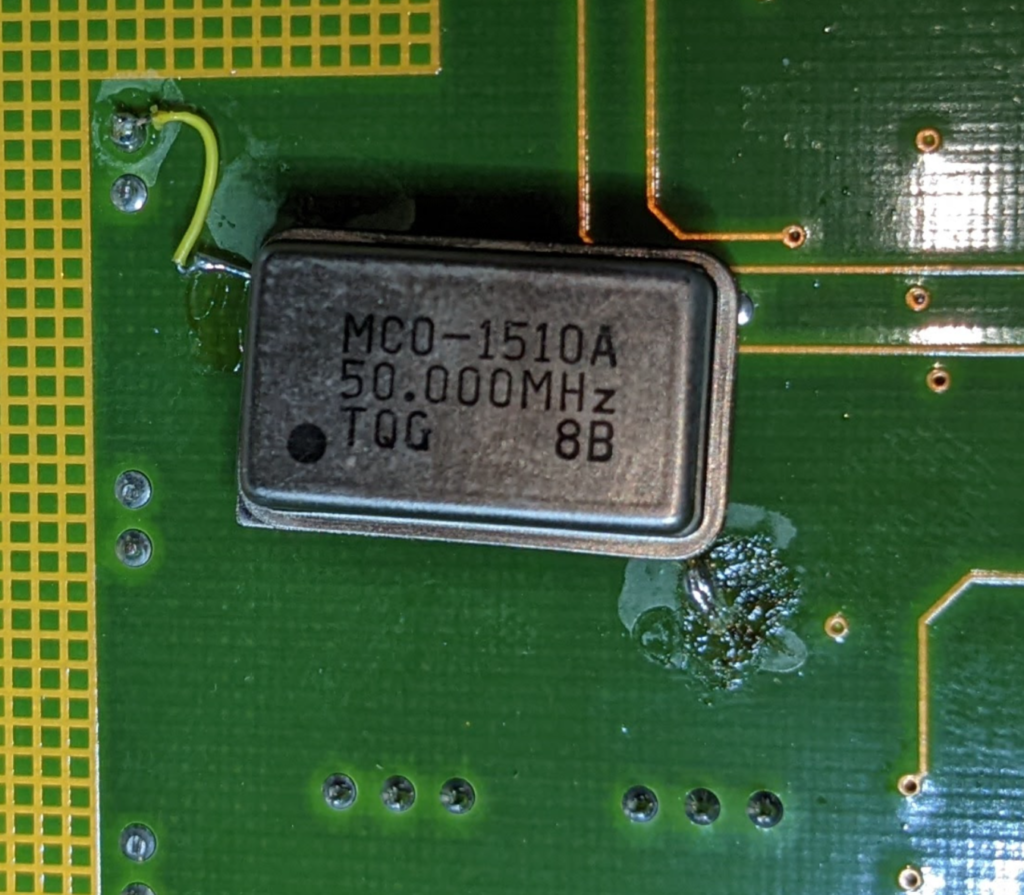
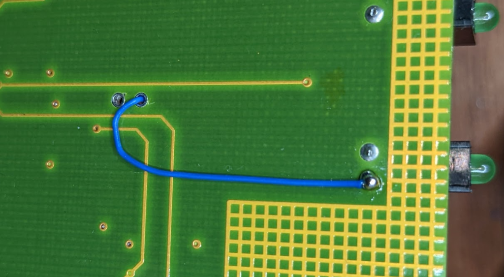
Flipping the board over we find a 50MHz crystal can powered by the +5v side of an LED, clock out through the X! via and ground to a random graound via.
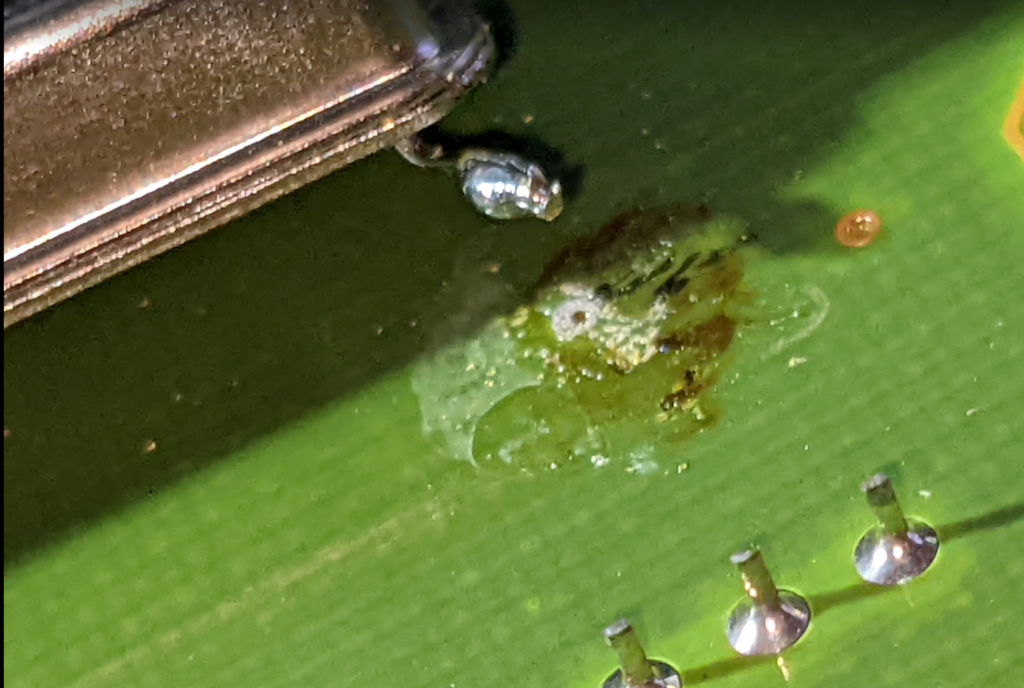
looking more closley at it, the poor soldering job to the gound VIA
Relocating the Clock
Removing the bodge works and cleaning up everything.
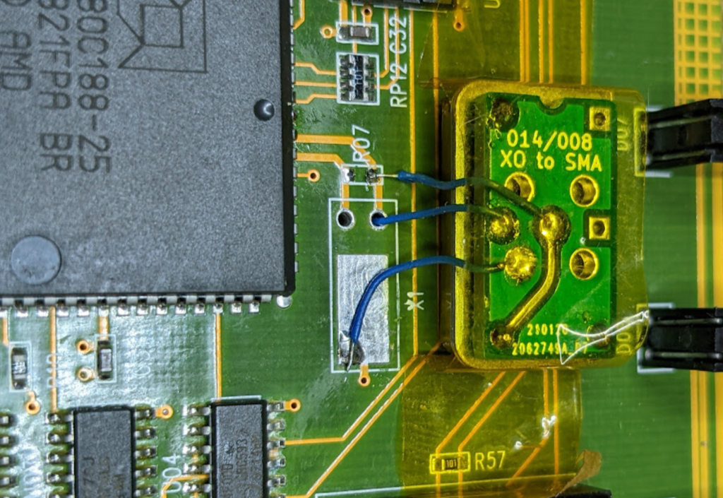
Xo carrier should anyone want one
https://github.com/hegars/14DIPxSMA
Remounted the clock onto a carrier board for easy soldering and connecting it to all the pads
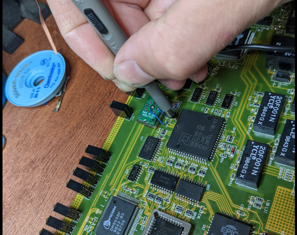
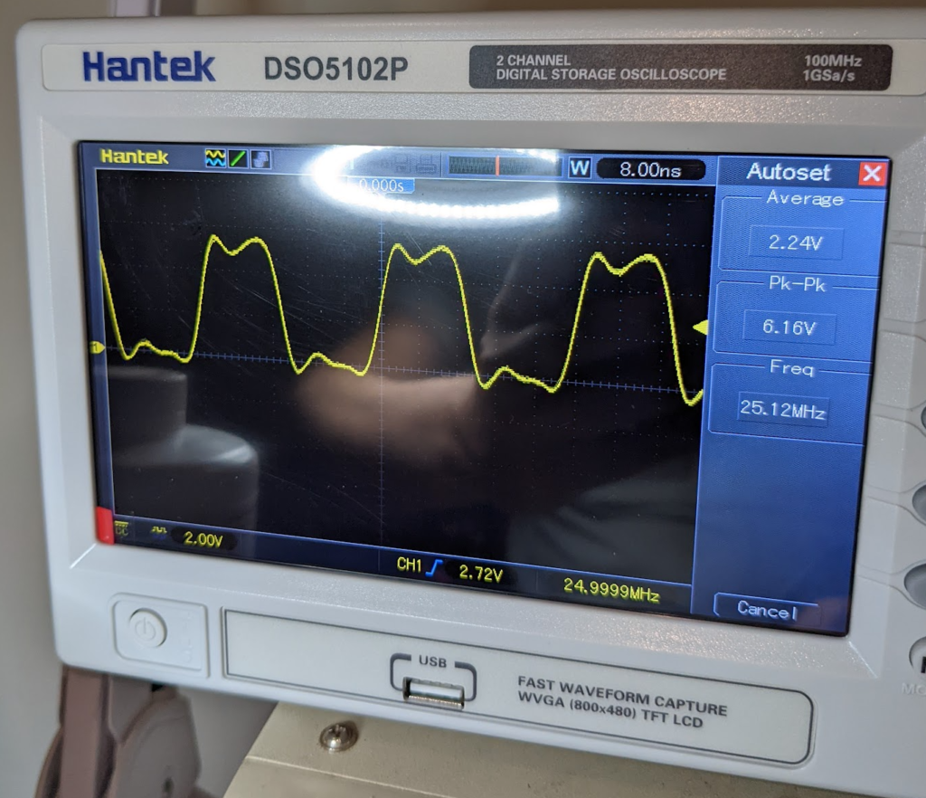
Testing Clock out
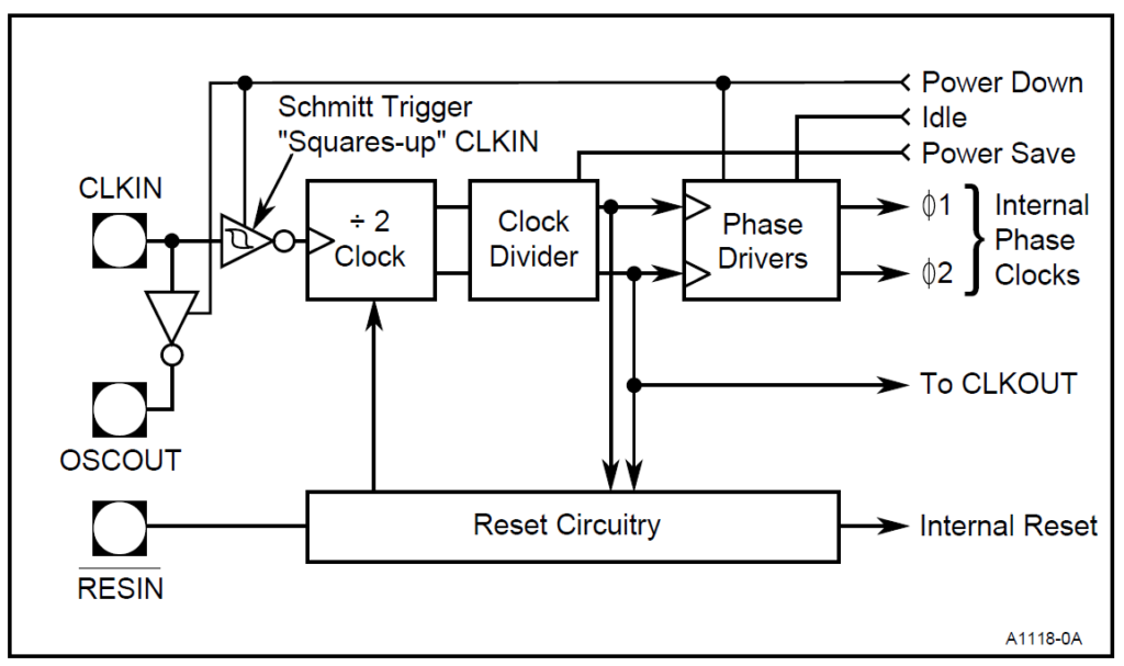
The CPU was now getting warm and the clock drive is 50Mhz to PIN 59 (X1) it is divided by 2 by the CPU and then ouput on PIN 56 (CLKOUT) giving 25MHz
EEPROM
Removing the eeprom, reading it and putting a socket on
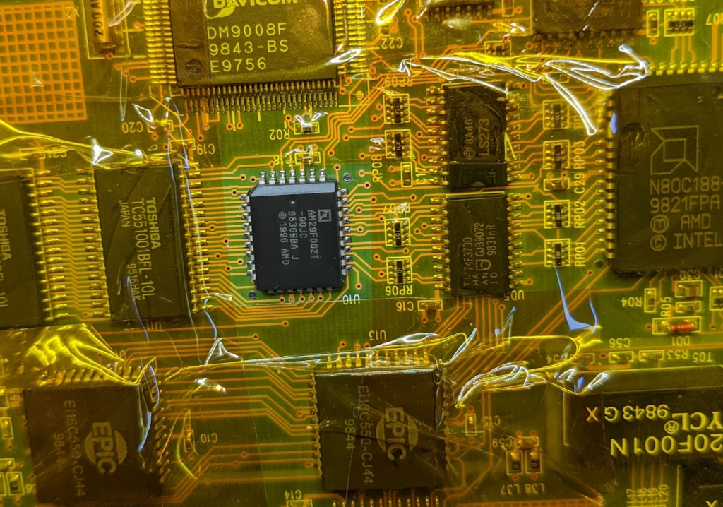
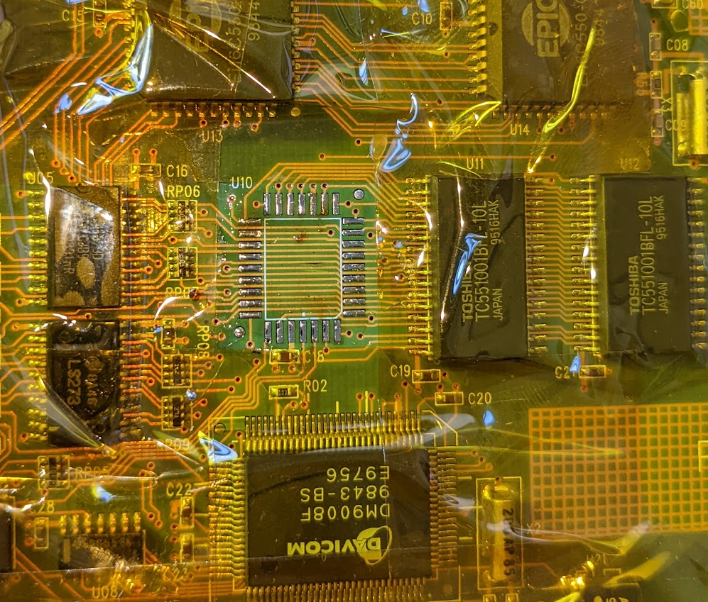
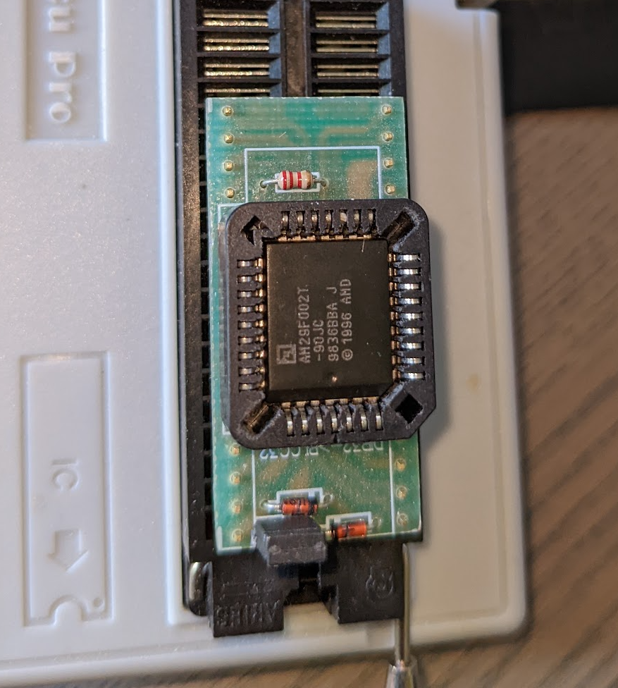
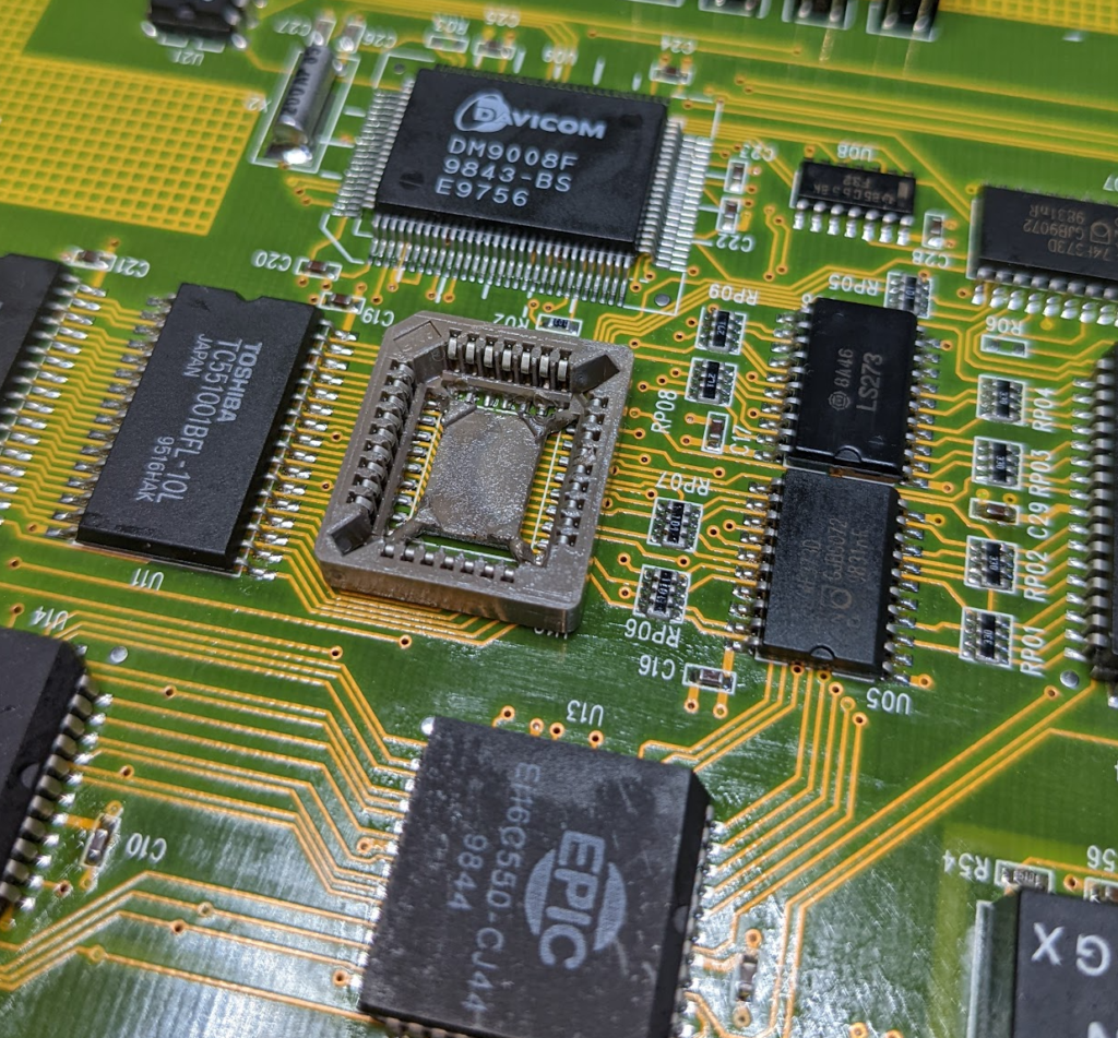
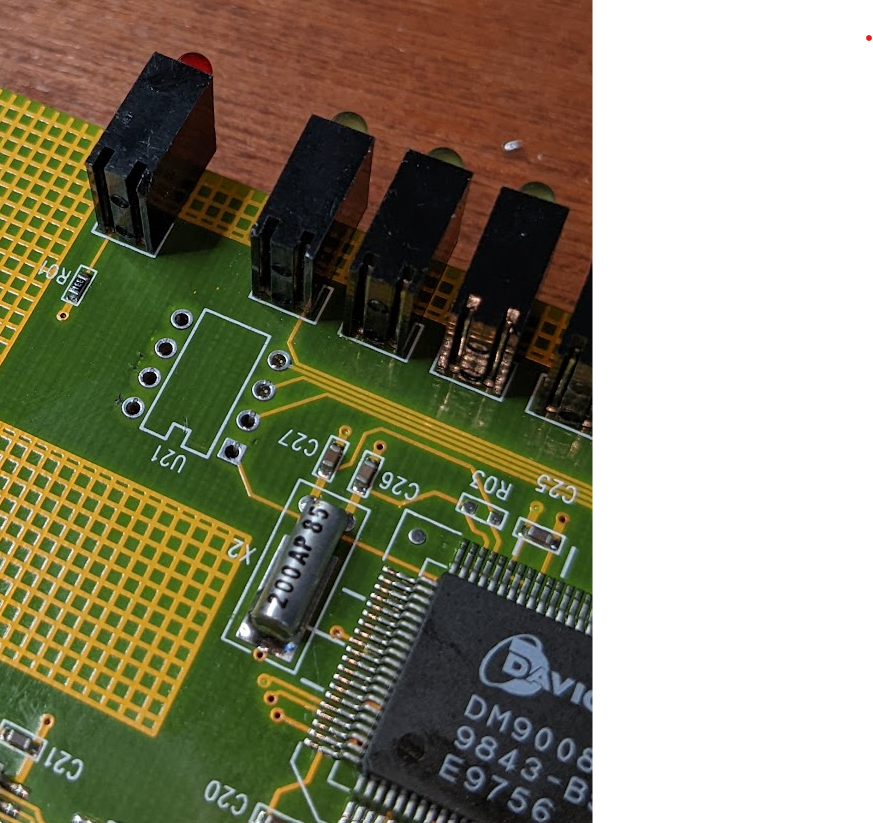
Socketing the NIC Serial eeprom
Socketing the serial EEPROM from the network card for science.
Also this is a 20MHz clock
Replacing the Magnetics to the Network card
The Magnetics from the CPU’s network card off the the HUB looked a bit melted, could have been from a soldering iron but it was work replacing the 1998 part with the newer 2016 part 20F991N -> 20F001NG (G for RoHS i think)
Memory Part
Serial Outputs
Serial clock marked 737AT3Z which is a 7.3728 MHz clock for BAUD generation
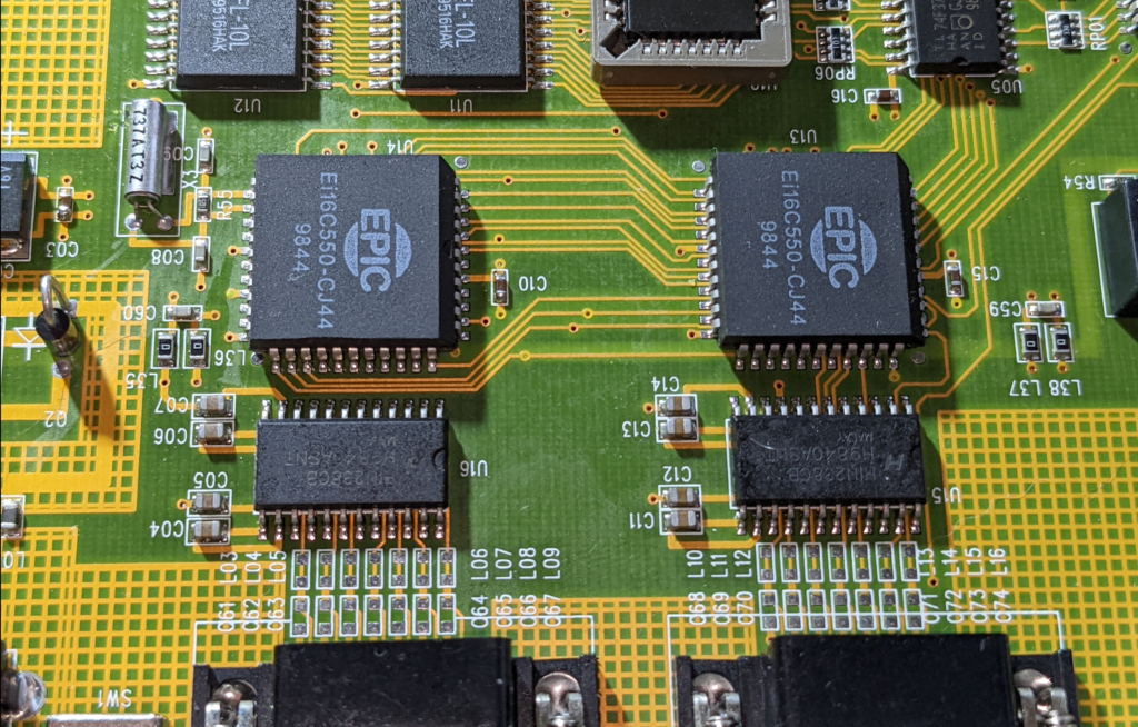
What is the highest baud rate produced by an internal clock? The highest baud rate is an X1 clock input divided by 16. For xample: At 3.6864Mhz, the highest baud rate is 3.6864M/16 = 230.4K baud. At 8Mhz, the highest baud rate is 8M/16 = 500K baud. What is the maximum baud rate in timer mode with a crystal of 3.6864Mhz? The maximum baud rate is a C/T clock input divided by 64. For example, at 3.6864Mhz, the maximum baud rate is 3.6864M/(2162) = 57.6K baud. If the crystal of 3.6864Mhz is doubled, will the baud rates in each column in the baud rate selection table be doubled? Yes. For example, if a crystal of 7.3728Mhz (2*3.6864Mhz) is used, the baud rates will be doubled as follows: The 57.6K and 115.2K in one column will become 115.2K and 230.4K